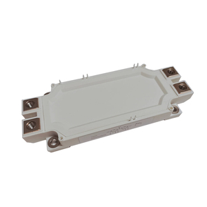

Explore our certified OEM/ODM Silicon Carbide (SiC) MOSFETs, Schottky Diodes, and advanced ceramic filtration modules designed for high-density power conversion and critical industrial environments.
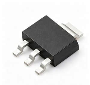
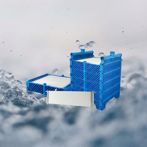
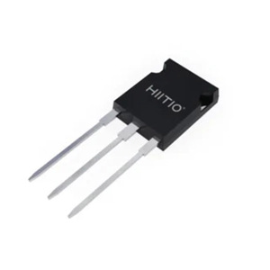
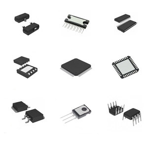
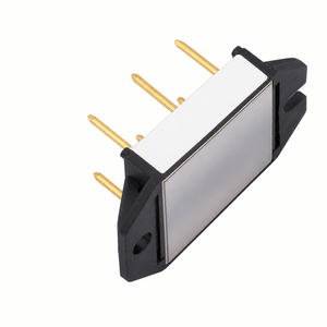
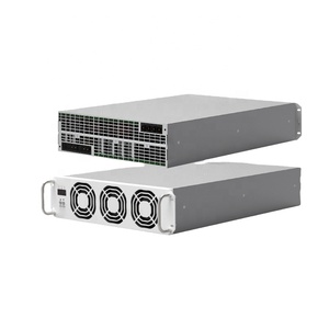
Headquartered in Barcelona, Spain, our engineering team de-risks power conversion programs by pairing state-of-the-art Wide Bandgap (WBG) Silicon Carbide substrate technology with decades of field-proven design standards.
From raw SiC die selection to specialized pin-fin substrate metallization, our Barcelona R&D center transforms challenging mechanical, electrical, and thermal constraints into serial-manufacturable power hardware.









The transition from traditional Silicon (Si) Insulated Gate Bipolar Transistors (IGBTs) to wide-bandgap Silicon Carbide (SiC) MOSFET power modules represents a fundamental paradigm shift in modern power electronics. As energy conversion demands reach unprecedented efficiency thresholds ($>99\%$), industrial applications ranging from 800V Electric Vehicle DC Fast Chargers (DCFC) to 1200V–3300V traction inverters require semiconductors capable of operating at higher junction temperatures ($T_j \ge 175^\circ\text{C}$), elevated switching frequencies ($>100\text{ kHz}$), and significantly reduced specific on-resistance ($R_{DS(on)}\cdot A$).
Silicon Carbide is a compound semiconductor featuring a bandgap energy of approximately $3.26\text{ eV}$—nearly triple that of standard Silicon ($1.12\text{ eV}$). This wide energy bandgap imparts extraordinary critical breakdown field strength ($E_{crit} \approx 3.0\text{ MV/cm}$ compared to $0.3\text{ MV/cm}$ for Si), permitting vastly thinner drift layers with higher doping concentrations for equivalent voltage ratings.
| Physical Property | Silicon (Si) | 4H-Silicon Carbide (4H-SiC) | Gallium Nitride (GaN) | System Level Impact |
|---|---|---|---|---|
| Bandgap Energy ($E_g$, eV) | 1.12 | 3.26 | 3.40 | Substantially lower intrinsic carrier concentration; stable high-temperature performance. |
| Breakdown Field ($E_{crit}$, MV/cm) | 0.30 | 3.00 | 3.30 | Allows 10x thinner drift layer; reduces $R_{DS(on)}$ and conduction losses. |
| Thermal Conductivity ($k$, W/cm·K) | 1.50 | 4.90 | 1.30–2.00 | Superior heat dissipation; reduced heatsink size & simplified thermal management. |
| Electron Saturation Velocity ($v_{sat}, 10^7\text{cm/s}$) | 1.00 | 2.00 | 2.50 | Enables rapid switching speeds; dramatically lowers switching energy ($E_{on}, E_{off}$). |
Because SiC MOSFETs switch in nanoseconds with extreme current rates of change ($di/dt > 10\text{ A/ns}$), conventional wire-bonded power packages introduce transient voltage spikes given by $V_{spike} = L_\sigma \cdot (di/dt)$. Overcoming this challenge requires advanced OEM packaging architectures:
Active Metal Brazing (AMB) Silicon Nitrides ($\text{Si}_3\text{N}_4$) offer exceptional mechanical toughness and thermal conductivity, enduring rigorous thermal cycling between $-55^\circ\text{C}$ and $+175^\circ\text{C}$ without delamination.
Replacing conventional Pb-based liquid solder with pressure silver sintering improves thermal resistance ($R_{th(j-c)}$) by up to 40% and raises operating fatigue thresholds by 5x to 10x.
Integrating dedicated Kelvin source pins decouples gate control loops from power path parasitic inductance, eliminating gate oscillation and ensuring clean $V_{GS}$ driving.
Custom OEM power modules tailored for harsh operating environments, ultra-high temperature profiles, and maximum system availability.
Enabling high-power 40kW to 360kW DC Fast Chargers (DCFC) with 1200V SiC MOSFETs. Slashes converter volume by 40% while achieving $>98.5\%$ peak efficiency in bi-directional V2G chargers.
Powering auxiliary power units (APU), catenary DC/AC inverters, and traction auxiliary systems. Fully tested for wide input range surges, shock, and extreme thermal cycling.
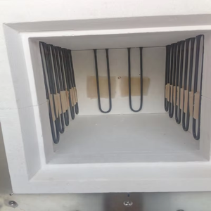
Silicon Carbide embedded ceramic heating modules engineered for high thermal stability in furnace chambers up to $1600^\circ\text{C}$, offering uniform heat emission and high energy density.
The industry shift from 150mm (6-inch) to 200mm (8-inch) 4H-SiC wafer fabrication is projected to yield a 20-30% reduction in die cost by 2027. Procurement managers should align with OEMs capable of supporting multi-wafer-size sourcing to ensure cost-competitiveness.
Global geopolitical tensions and raw material allocation make supply chain transparency vital. Leading B2B buyers now mandate dual-source substrate qualification, pin-compatible package alternatives, and transparent long-term component lifecycle roadmaps.
Next-gen procurements favor Intelligent Power Modules (IPMs) that co-package isolated gate drivers, temperature sensors ($NTC/PTC$), and desaturation ($DESAT$) short-circuit protection circuits directly onto the AMB substrate, reducing system NRE time.